- 您现在的位置:买卖IC网 > Sheet目录377 > 2N7002KW (Fairchild Semiconductor)MOSFET N-CH 60V 310MA SOT323
May 2011
2N7002KW
N-Channel Enhancement Mode Field Effect Transistor
Features
?
?
?
?
?
?
?
?
Low On-Resistance
Low Gate Threshold Voltage
Low Input Capacitance
Fast Switching Speed
Low Input/Output Leakage
Ultra-Small Surface Mount Package
Pb Free/RoHS Compliant
ESD HBM=1000V as per JESD22 A114 and ESD CDM=1500V as per JESD22 C101
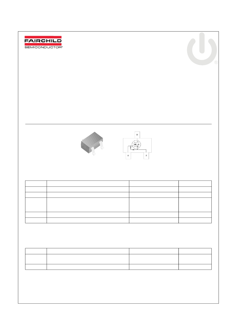
D
S
G
SOT-323
Marking : 7KW
Absolute Maximum Ratings *
T A = 25°C unless otherwise noted
Symbol
V DSS
V GSS
Parameter
Drain-Source Voltage
Gate-Source Voltage
Value
60
±20
Units
V
V
I D
Maximum Drain Current
- Continuous
T J = 100 ° C
- Pulsed
310
195
1.2
mA
mA
A
T J
T STG
Operating Junction Temperature Range
Storage Temperature Range
-55 to +150
-55 to +150
° C
° C
* These ratings are limiting values above which the serviceability of any semiconductor device may by impaired.
Thermal Characteristics
Symbol
P D
R θ JA
Parameter
Total Device Dissipation
Derating above T A = 25°C
Thermal Resistance, Junction to Ambient *
Value
300
2.4
410
Units
mW
mW/ ° C
° C/W
* Device mounted on FR-4 PCB, 1 inch x 0.85 inch x 0.062 inch. Minimum land pad size
? 2011 Fairchild Semiconductor Corporation
2N7002KW Rev. A0
1
www.fairchildsemi.com
发布紧急采购,3分钟左右您将得到回复。
相关PDF资料
2N7002K
MOSFET N-CH 60V 115MA SOT23
2N7002LT1
MOSFET N-CH 60V 115MA SOT-23
2N7002T-7
MOSFET N-CH 60V 115MA SOT-523
2N7002TC
MOSFET N-CHAN 60V SOT23-3
2N7002T
MOSFET N-CH 60V 115MA SOT-523F
2N7002VA
MOSF N CH DL 60V 280MA SOT 563F
2N7002VC-7
MOSFET N-CH DUAL 60V SOT-563
2N7002W-7
MOSFET N-CH 60V 115MA SOT-323
相关代理商/技术参数
2N7002KW _R1 _00001
制造商:PanJit Touch Screens 功能描述:
2N7002KW_ R2 _00001
制造商:PanJit Touch Screens 功能描述:
2N7002KW_10
制造商:PANJIT 制造商全称:Pan Jit International Inc. 功能描述:60V N-Channel Enhancement Mode MOSFET - ESD Protected
2N7002KW-TP
制造商:Micro Commercial Components (MCC) 功能描述:Trans MOSFET N-CH 60V 0.34A 3-Pin SOT-323 T/R
2N7002L
制造商:ONSEMI 制造商全称:ON Semiconductor 功能描述:Small Signal MOSFET 60 V, 115 mA, N−Channel SOT−23
2N7002L_10
制造商:UTC-IC 制造商全称:UTC-IC 功能描述:60V, 115mA, N-CHANNEL MOSFET
2N7002L_12
制造商:ONSEMI 制造商全称:ON Semiconductor 功能描述:Small Signal MOSFET 60 V, 115 mA, N.Channel SOT.23
2N7002L6327HTSA1
制造商:Infineon Technologies AG 功能描述:Trans MOSFET N-CH 60V 0.3A 3-Pin SOT-23 T/R 制造商:Infineon Technologies AG 功能描述:MOSFET N-CH 60V 300MA SOT-23
